Description
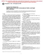
1.1 These test methods provide means for examining the edge contour of circular wafers of silicon, gallium arsenide, and other electronic materials, and determining fit to limits of contour specified by a template that defines a permitted zone through which the contour must pass. Principal application of such a template is intended for, but not limited to, wafers that have been deliberately edge shaped.
1.2 Two test methods are described. One is destructive and is limited to inspection of discrete points on the periphery, including flats. The contour of deliberately edge-shaped wafers may not be uniform around the entire periphery, and thus the discrete location(s) may or may not be representative of the entire periphery. The other test method is nondestructive and suitable for inspection of all points on the wafers periphery except flats.
1.3 The nondestructive test method may also be applied to the examination of the edge contour of the outer periphery of substrates for rigid disks used for magnetic storage of data.
Note 1 – Reference to wafers in the remainder of this standard shall be interpreted to include substrates for rigid disks unless the phrase “of electronic materials” is also included in the context.
1.4 The values stated in SI units are to be regarded as the standard. The values given in parentheses are for information only.
1.5 This standard does not purport to address all of the safety concerns, if any, associated with its use. It is the responsibility of the user of this standard to establish appropriate safety and health practices and determine the applicability of regulatory limitations prior to use.
Product Details
- Published:
- 01/01/1999
- Number of Pages:
- 4
- File Size:
- 1 file , 29 KB


